
Fast producing Flexible PCB Manufacturing FPC
Product Description
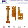
Fast Producing FPC Manufacturing Flex PCB/ Flexible PCB
Flexible Printed Circuit Board, commonly known as FPC, is a printed circuit board made of flexible insulating substrates (mainly polyimide or polyester film), which has many advantages that hard printed circuit boards do not have. For example, it can bend, roll and fold freely. The volume of electronic products can be greatly reduced by using FPC, which is suitable for the development of electronic products in the direction of high density, miniaturization and high reliability. Therefore, FPC has been widely used in aerospace, military, mobile communications, laptop computers, computer peripherals, PDA, digital cameras and other fields or products.

FPC also has the advantages of good heat dissipation and weldability, easy assembly and low comprehensive cost.
Flexible printed circuit boards can be divided into single-sided flexible PCB, double-sided flexible PCB and multi-layer flexible PCB boards. Polyimide copper clad laminates are the main substrates used. This material has high heat resistance, good dimensional stability, and the final product is made by pressing the covering film with both mechanical protection and good electrical insulation. The surface and inner conductors of double-sided and multi-layer printed circuit boards are metallized to realize the electrical connection between the inner and outer circuits.
And Rigid PCB is a completely different product from flexible PCB. However, flexible circuit boards and rigid circuit boards have a perfect combination, forming rigid- flex circuit boards, we can see in many application scenarios.
")
We can provide one-stop service:
1. Quick and Fast producing Manufacturing Flexible PCB
2. PCB circuit boards.
3. E-test.
4.Electronic components purchasing.
5. PCB assembly services: available on SMT, BGA, DIP.
6. PCBA function test.
7. Enclosure assembly.
PCB product Capacity
| PCB Manufacture Capacity | |
| Item | Specification |
| Material | FR-4, FR1,FR2; CEM-1, CEM-3,Rogers, Teflon,Arlon,Aluminum Base, Copper Base,Ceramic, Crockery, etc. |
| Remarks | High Tg CCL is Available(Tg>=170℃) |
| Finish Board Thickness | 0.2 mm-6.00mm(8mil-126mil) |
| Surface Finish | Gold finger(>=0.13um), Immersion Gold(0.025-0075um), Plating Gold(0.025-3.0um), HASL(5-20um), OSP(0.2-0.5um) |
| Shape | Routing,Punch,V-cut,Chamfer |
| Surface Treatment | Solder Mask(black, green, white, red, blue, thickness>=12um, Block, BGA) |
| Silkscreen(black, yellow, white) | |
| Peel able-mask(red, blue, thickness>=300um) | |
| Minimum Core | 0.075mm(3mil) |
| Copper Thickness | 1/2 oz min; 12oz max |
| Min Trace Width & Line Spacing | 0.075mm/0.075mm(3mil/3mil) |
| Min Hole Diameter for CNC Drilling | 0.1mm(4mil) |
| Min Hole Diameter for Punching | 0.6mm(35mil) |
| Biggest panel size | 610mm * 508mm |
| Hole Position | +/-0.075mm(3mil) CNC Drilling |
| Conductor Width(W) | +/-0.05mm(2mil) or +/-20% of original |
| Hole Diameter(H) | PTHL:+/-0.075mm(3mil) |
| Non PTHL:+/-0.05mm(2mil) | |
| Outline Tolerance | +/-0.1mm(4mil) CNC Routing |
| Warp & Twist | 0.70% |
| Insulation Resistance | 10Kohm-20Mohm |
| Conductivity | <50ohm |
| Test Voltage | 10-300V |
| Panel Size | 110 x 100mm(min) |
| 660 x 600mm(max) | |
| Layer-layer misregistration | 4 layers:0.15mm(6mil)max |
| 6 layers:0.25mm(10mil)max | |
| Min spacing between hole edge to circuitry pattern of an inner layer | 0.25mm(10mil) |
| Min spacing between board outline to circuitry pattern of an inner layer | 0.25mm(10mil) |
| Board thickness tolerance | 4 layers:+/-0.13mm(5mil) |
Flexible PCB product Capacity
| FPC Tech Specification | |
| Items | Capabilities |
| Layers | FPC:1 to 6 Layers, Rigid Flex: 2 to 10 Layers |
| Regular Base Materials | Kapton,Polyimide(PI), Polyester(PET), FR4 |
| Base Copper Thickness | 1/3 oz to 8oz |
| Regular Base Material Thickness | 12.5um to 50um(FPC) |
| 0.1mm to 3.2mm(Rigid) | |
| Regular Coverlay Thickness | 27um to 50um |
| Regular Adhesive Thickness | 12um to 25um |
| Blind or Buried Vias | Yes |
| Impedance Control | Yes |
| Min.Line Width/Spacing | 0.04mm/0.04mm |
| Surface Finishing | Electroplate Ni/Au(Flash gold/Soft gold/Hard gold), ENIG, HASL, Immersion Tin,OSP |
| Outline Fabrication | Die cut, laser cut, CNC routing, V-scoring |
| Hole to edge(Hard tool/Die Cut) | ±0.1/±0.2mm |
| Edge to edge(Hard tool/Die Cut) | ±0.05/±0.2mm |
| Circuit to edge(Hard tool/Die Cut) | ±0.07/±0.2mm |
PCB Assembly(SMT) Product Capacity
| SMT Capacity | |
| SMT Item | Capacity |
| PCB Max. size | 510mm*1200mm(SMT) |
| Chip component | 0201, 0402, 0603, 0805, 1206 package |
| Min.pin space of IC | 0.1mm |
| Min. space of BGA | 0.1mm |
| Max.precision of IC assembly | ±0.01mm |
| Assembly capacity | ≥8 million piots/day |
| DIP capacity | 6 DIP production lines |
| Assembly testing | Bridge test,AOI test, X-Ray test, ICT(In Circuit Test),FCT(Functional Circuit Test) |
| FCT(Functional Circuit Test) | Current test, voltage test, high temperature and low temperature test,Drop Impact Test,aging test,water proof test,leakage-proof test and etc.Different test can be done according to your requirement. |
Product Categories : Flexible PCB